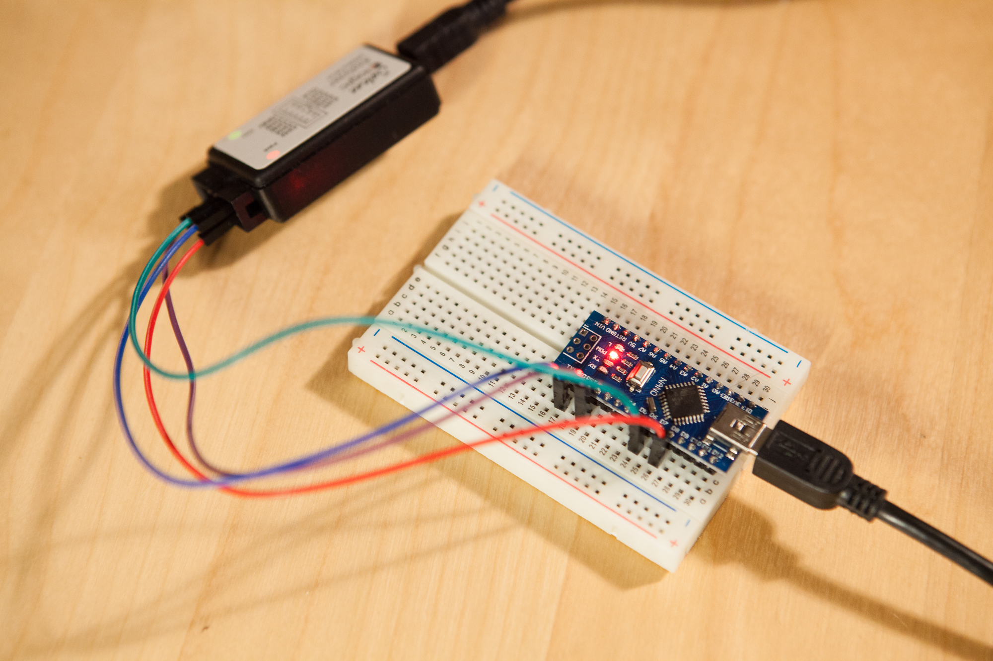
So far the hardware side of the Adalight setup has been a nest of wires on my desk, with the Arduino on a breadboard and the power running through a terminal block. Now it’s time to wrap up this project by getting everything off of the breadboard and onto a dedicated PCB in its own custom case!
This post is part of a series on creating a DIY ambilight using Adalight and WS2812B LEDs. Check out the project page here.
Designing a PCB for Adalight
I’ve never designed or made a custom printed circuit board (PCB) before, so I wanted to keep things simple.
From a hardware perspective this project is actually pretty basic. For a barebones setup, all you need is the LED strip (which comes with WS2812B LEDs and 0.1 µF capacitors), an Arduino, and a 5 V power supply that can provide enough amperage. Since the LED strip is self-contained, all the PCB needs to do is house the Arduino and source the 5 V power.
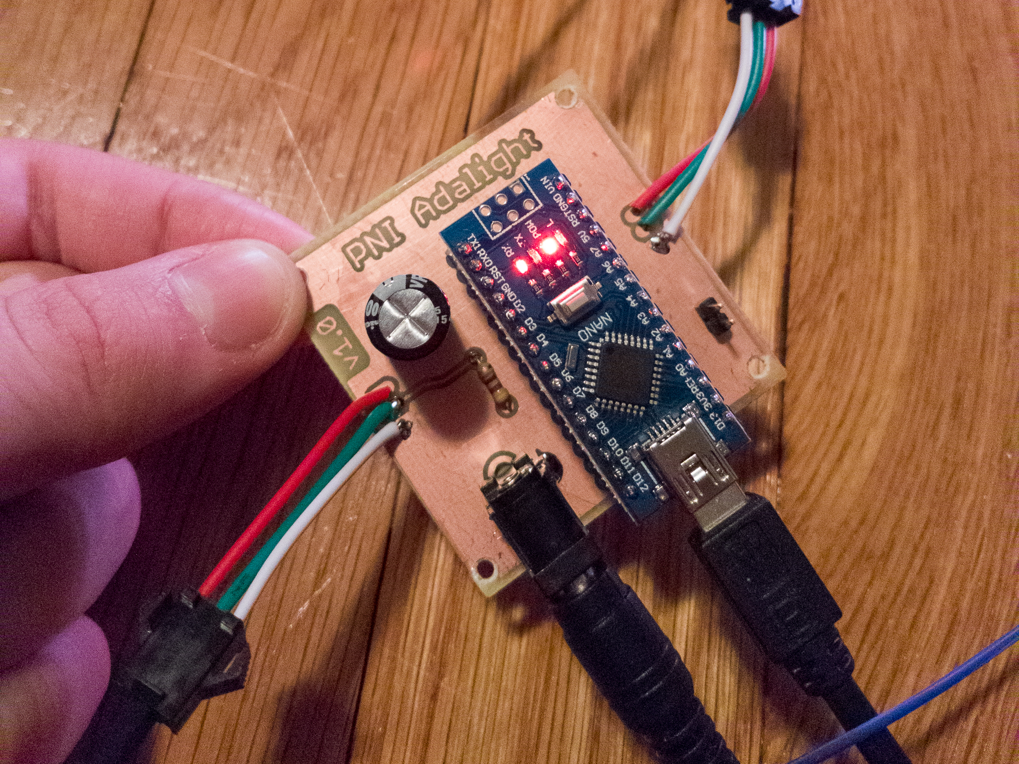
In the interest of keeping things simple, I decided to use a pre-built Arduino Nano and some female headers rather than building my own circuit with a standalone ATMEGA chip. In addition to the Arduino, I added a 470 Ω resistor in series with the data line to prevent the strip from drawing power via USB and a 1000 µF capacitor to smooth power from the external power supply. Because the Arduino’s built-in reset button is going to be hidden in the case, I also added a 2-pin header for an optional external reset button.
EAGLE CAD: Building the Schematic
This was my first time using EAGLE, and I found it surprisingly easy to pick up. I followed SparkFun’s EAGLE tutorials, which are quite well written and easy to follow.
Similar to the way mechanical CAD programs use 2D sketches as a base for 3D extrapolation, EAGLE uses an electrical schematic as a base for creating a board layout.
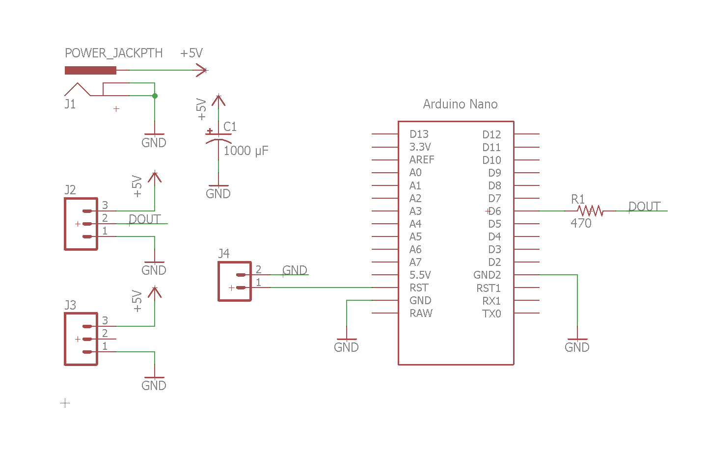
The first step was to insert all of the individual parts into the schematic. For this board, there are only a handful of components:
- Arduino Nano
- Barrel power jack
- 3-pin JST connectors (2x)
- 1000 µF capacitor
- 470 Ω resistor
- 2-pin reset header
With all of the components added, I then used the ‘net’ tool to form the electrical connections. Positioning doesn’t matter, so place things in a way where the connections are easy to make. You can also use the ‘name’ tool to add connections between components anywhere on the schematic.
EAGLE CAD: Board Design
Clicking the “Generate/switch to board” button is where the real fun begins. All of the components in their proper footprints are moved to a layout area, with thin ‘airwires’ showing where the connections are supposed to go. From here it’s a puzzle: fit all of the components and traces in the smallest area while making the correct connections.
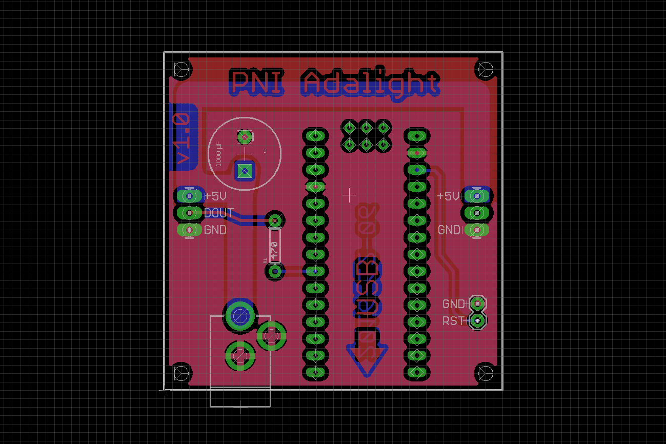
For any CAD, the place to start is with your limitations. That is to say: figure-out what you have to do, and build from there. With this PCB, I knew that the power jack and the Arduino’s USB port needed to face out the back so they were inline with the cables. I also wanted the two JST connections on either side of the board, so the pigtails coming off of the strip didn’t have to wrap around. Knowing those two things, I can place more than half of the components.
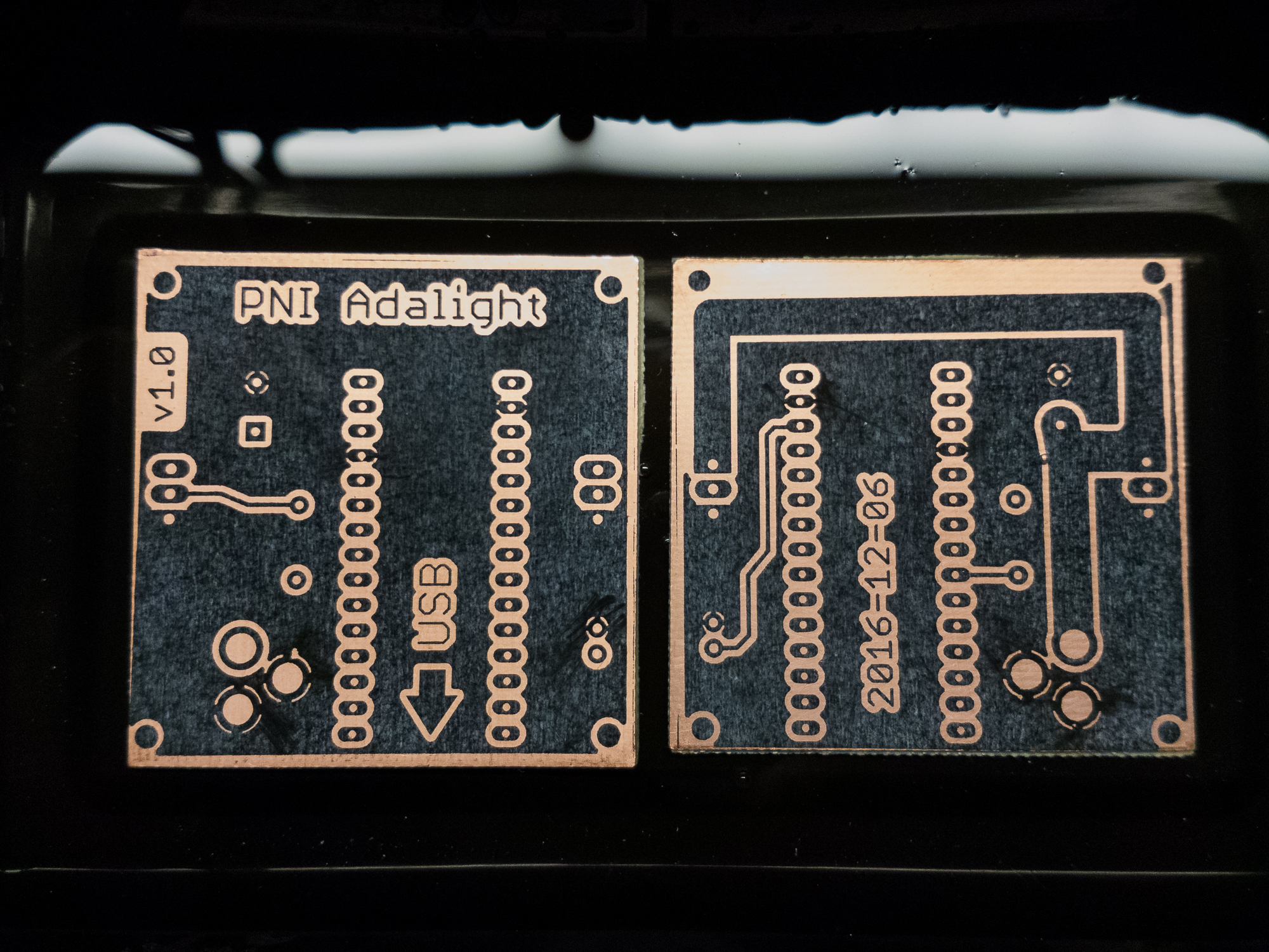
Because I’m etching this at home and I’ve never made a PCB before, I had a few additional limitations: for one, I didn’t want to use any vias to connect the two halves of the board. I also had no silkscreen to help guide component placement, so I needed to be wary of orientation and put important info on the copper itself.
Although it took longer than the schematic, the board design also went smoothly. I ended up with a 2×2″ PCB with M2 mounting holes on all four corners. Most of my time was spent playing with EAGLE’s polygons to get the traces to bend how I wanted them.
Copper PCB Etching at Home
There are a million-and-one guides on how to do DIY circuit board etching at home (I would know, I read a bunch of them before I tried!), so I’m not going to bother with an exhaustive step-by-step, but I will go through the basics and what worked for me.
Prepping the EAGLE Files
In EAGLE, I exported the Top, Bottom, and Pads layers as separate black and white images at 1200 DPI. I used Photoshop to composite the Pads layer with the Top/Bottom, and then inverted everything so the copper areas were black. I also covered over the Nano’s ICSP header, which is unnecessary for this board with the female headers. To finish it off, I flipped the Top layer so the printed version would apply to the copper at the correct orientation (the bottom layer is already flipped in EAGLE).
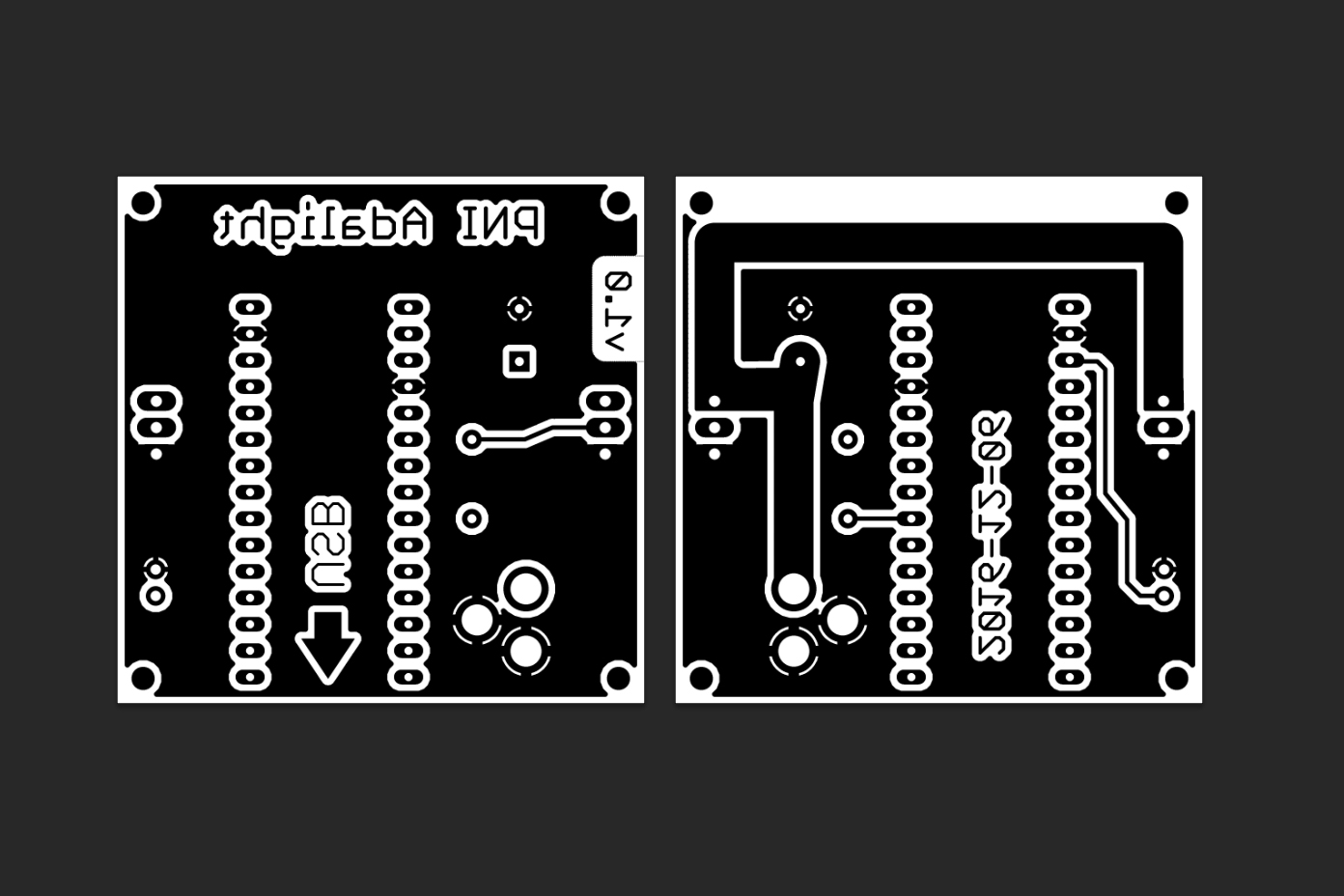
Copies of the black and white composites were arranged to fit on a standard 8.5 x 11″ sheet at 1:1 scale and then printed at high quality on glossy paper using a desktop laser printer.
Toner Transfer
After printing the design in black on a laser printer, I now had have a 1:1 copy of the copper areas for the PCB in a thin layer of printer toner. By transferring the toner to a copper-coated board, the copper underneath the toner is protected from the acid etching solution used to make the final PCB.
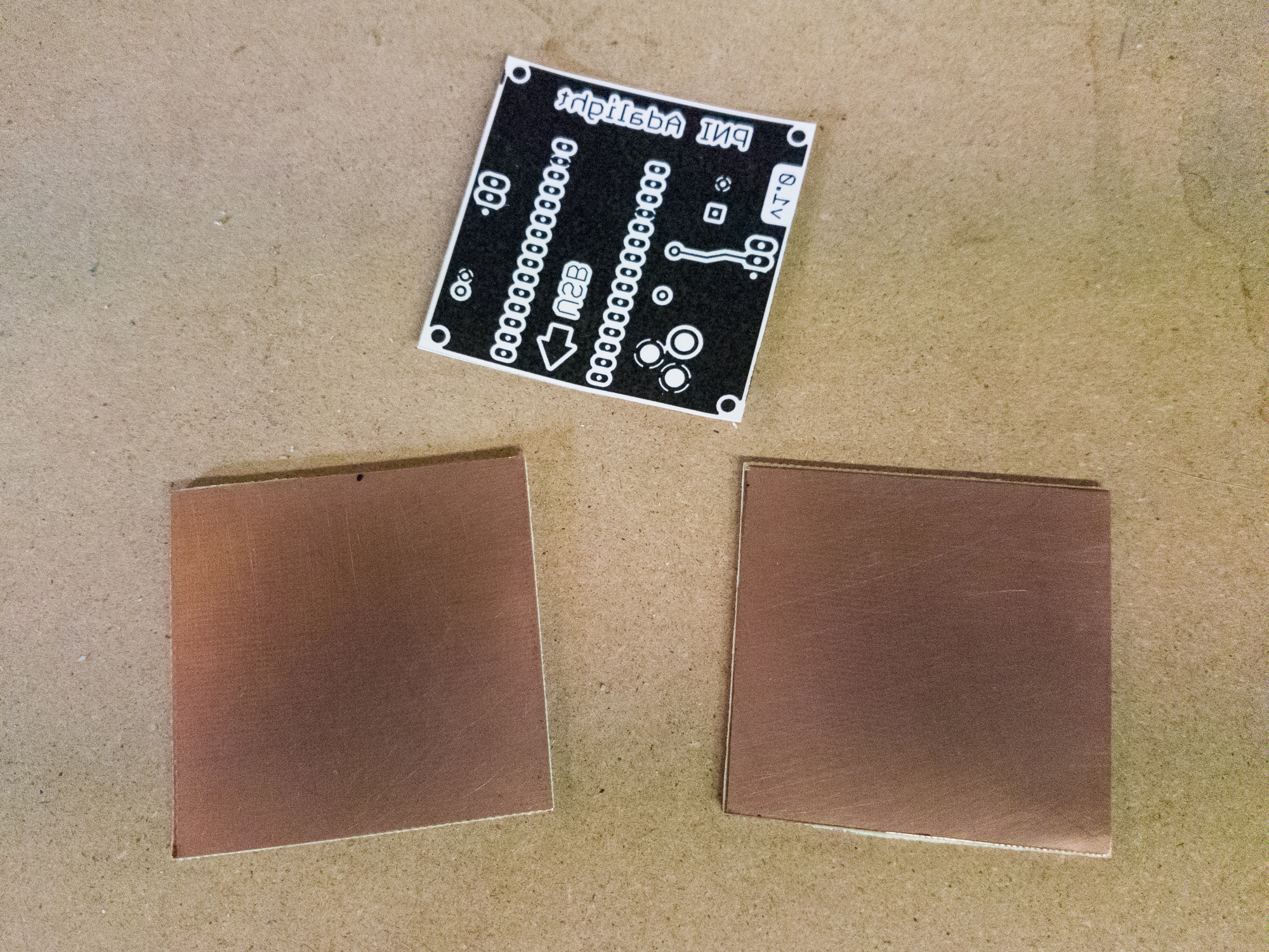
Since this was my first try making my own PCB, I purchased some inexpensive double-sided copper clad boards to play around with. These boards are just big enough for making two PCBs, so I decided to cut them before etching. Although they did end up working, their cheap quality showed itself when I went to trim them to size. I tried scoring and snapping the board, which caused the substrate to crack rather than snap. I ended up using a pair of heavy duty shears to cut them to size, which tore up the edges a bit but otherwise released very little dust (like cutting with a Dremel would have).
I sandwiched the printed paper between the copper board and a clothes iron to transfer the toner. The iron was set to its highest heat setting (no steam!), and held in place for 1 minute to get the toner to stick. I moved the iron around the board continuously for an additional 5 minutes, paying specific attention to the corners.
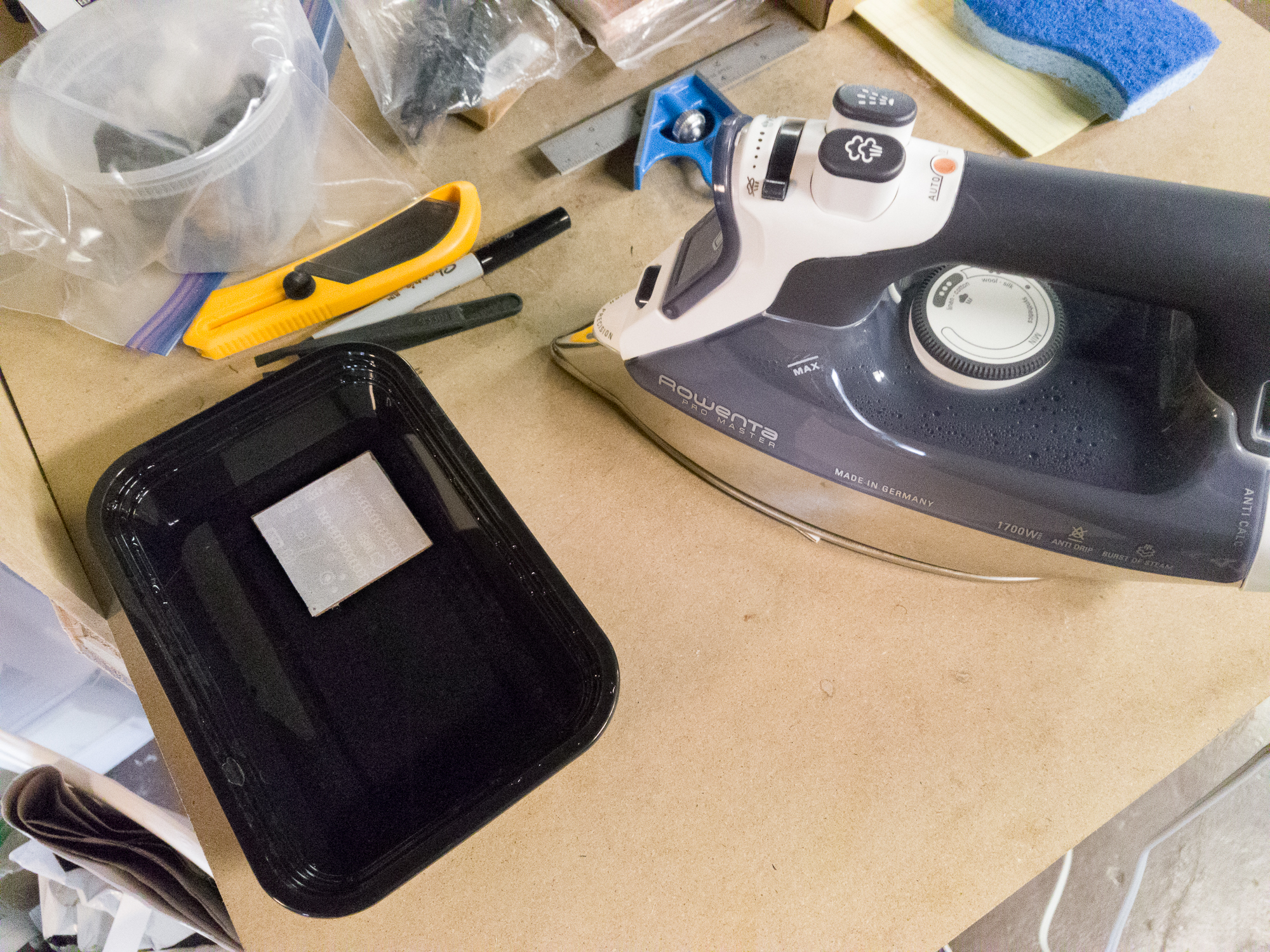
You can see a corner of one PCB sticking out from under the iron. The board on the left is sitting in a water bath to dissolve the paper.
After ironing, the board was dropped in water and left to soak for 10 minutes. The paper was then carefully peeled off and the residue wiped away using my fingers. The result was a near-perfect transfer of the toner onto the board!
Sponge-Etching
After washing off the remaining paper residue, it was time to etch. The design is for a double-sided board, and I decided to etch one side at a time. I transferred the design for only one side, and then covered the other side in packaging tape to protect it from the acid.
In my research for this, I found that the typical home etching method was to completely submerge the toner-covered board in an acid solution for around half an hour. This requires a lot of acid in a tub and takes a relatively long time.
I went with an alternate method, which was to use a sponge and dab the acid on the board. This requires a lot less acid and only takes about 5 minutes. Make sure to wear gloves and eye protection! I used a few ounces of ferric chloride to make both boards. The acid is pretty nasty, and in my cautious state I forgot to take a photo of the etching itself.
After etching, I thoroughly rinsed the boards and then drilled out the four mounting holes on each corner. I used the mounting holes to line up the design for the opposite side, and then repeated the toner transfer/sponge etching for the second side.

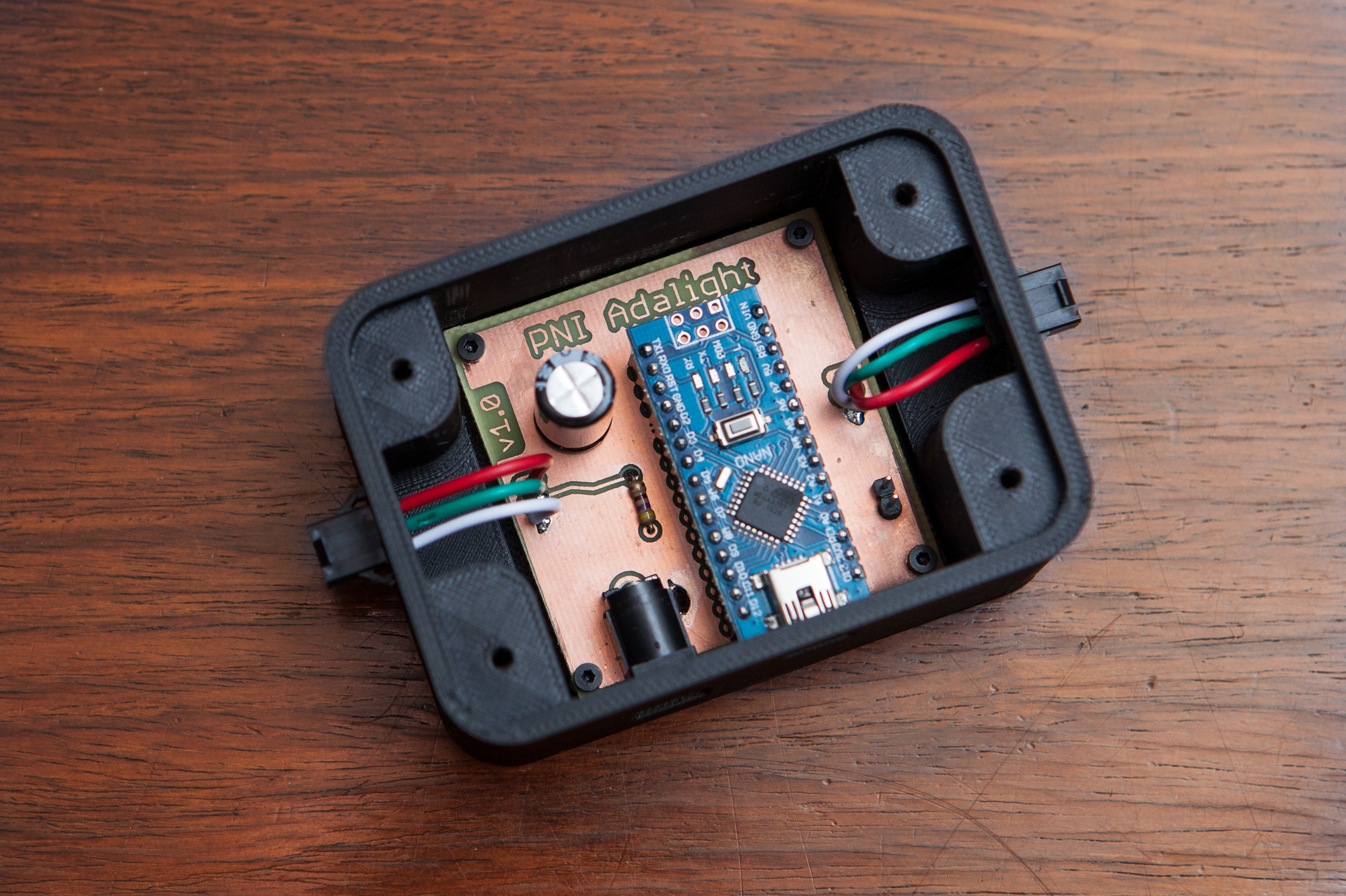
With everything etched, I used some acetone to clean off the toner and I was left with a circuit board! The last step was to take the board under a drill press and drill out all of the connections, and then solder the components in place. Voila! Homemade PCB!
Making a Custom Case
While I’ve never built a PCB before, I have a long and storied history of designing thingymajigs for 3D printing.
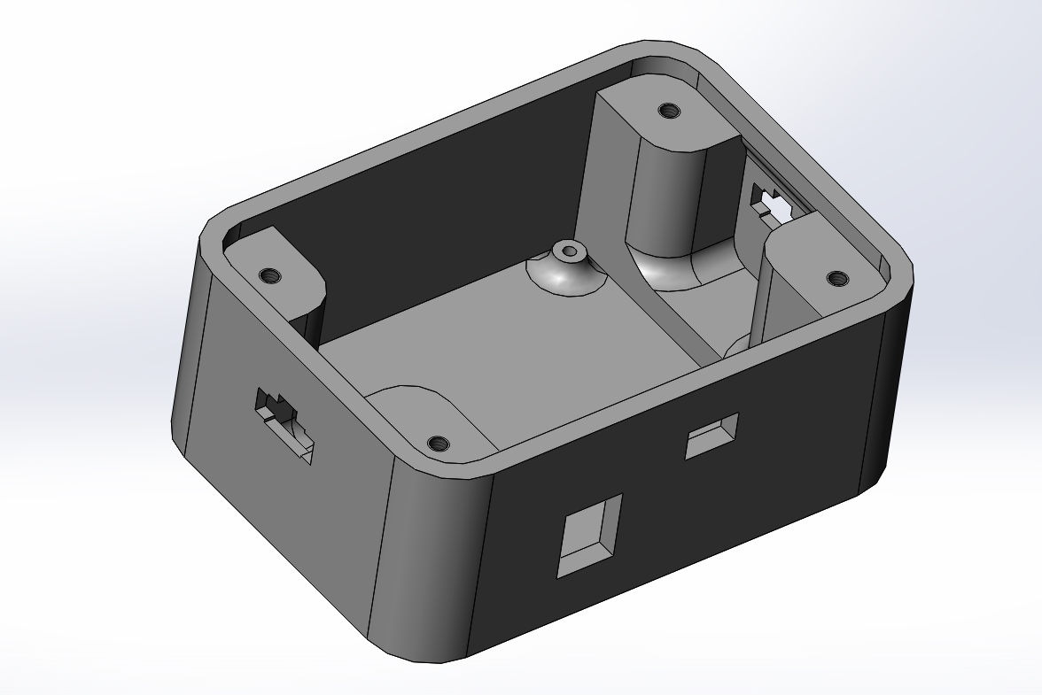
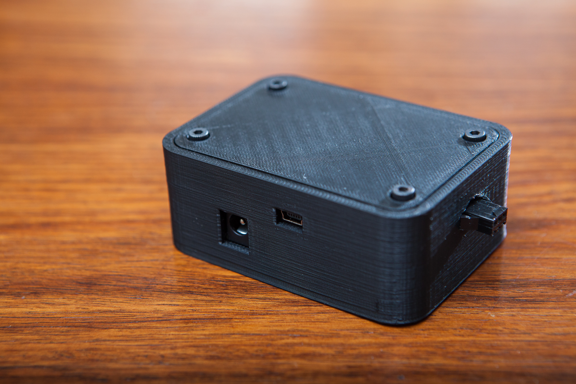
Continuing the theme of starting CAD with your known limitations: I know the exact dimensions of the board and the parts on it, so it’s just a matter of building a box around everything. I started with a 1/8″ base and added four printed M2 standoffs to the bottom for the PCB mounting. The walls were then built up above the level of the Arduino Nano and the tall capacitor, and built out far enough so the wires from the JST connectors would not be cramped. I also checked that the design would fit on the monitor stand, and that the pigtails from the LED strip would not be stressed.
I cut out a channel in the enclosure wall to the proper panel thickness for the JST connectors (1.75 mm), leaving the corners thick for strength and to support the top cover.
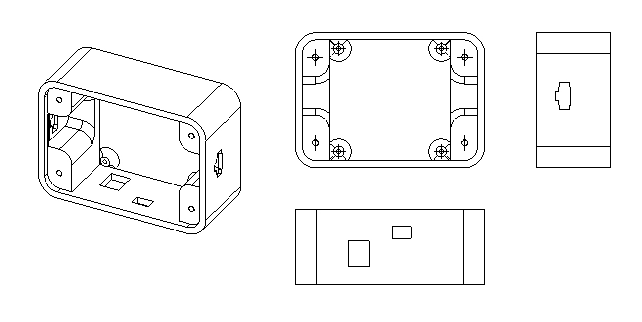
I exported the case as an STL and printed it out of Hatchbox ABS on my Printrbot. The case body took around 5 hours, and the lid took only 1. The case uses 4 M2 screws to attach the PCB and 4 M3 screws to attach the lid.
I forgot to add some extra room so the USB port could lift out of the enclosure, so the assembled PCB was a tight fit. I don’t think I’ll be able to get it out without cutting the case above the USB port, but that’s alright. I’ll need to update the CAD file for the next print.
Final Assembly
With the completed PCB and case, we can complete final assembly!
I cleaned off the back of the monitor and used 1″ velcro to attach the case to the monitor stand. While I was at it, I added a dab of hot glue to the base of the LED pigtails to keep them in place and prevent shorts.
I connected the LED pigtails to the connectors on the case. The pigtails are almost too short, but with the angle my monitor is at they reach without being in tension. If I end up making a version 2 of the PCB, I will definitely extend those leads an inch or two.
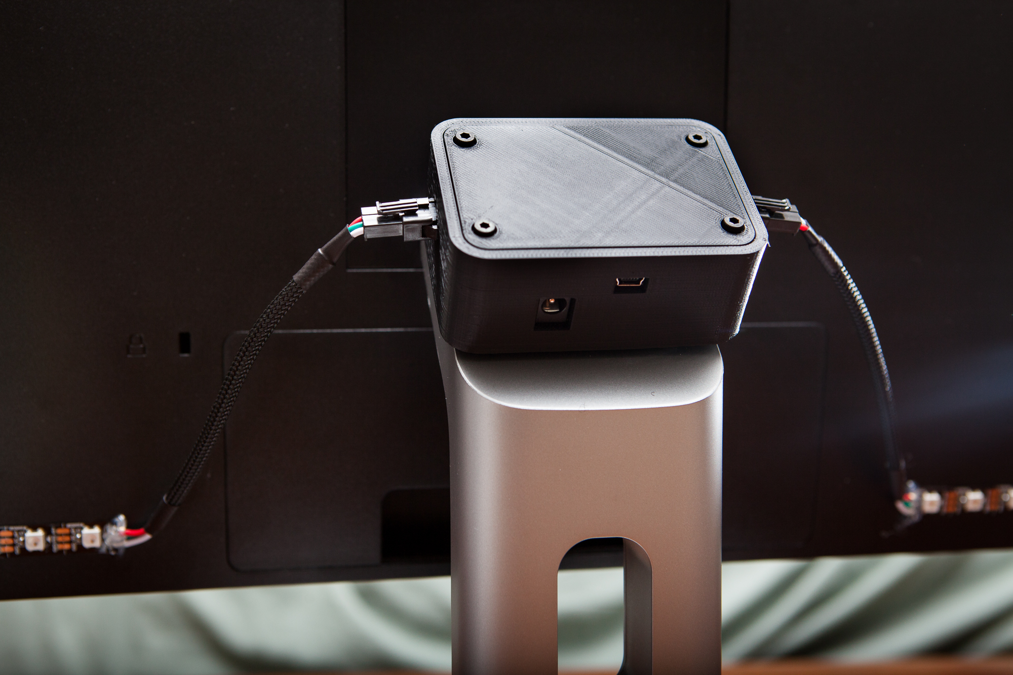
With everything in place, I put the monitor back on the desk and then routed the USB cable to the back of my desktop. I also used a few zip ties to hang the power supply underneath my desk.
Conclusion
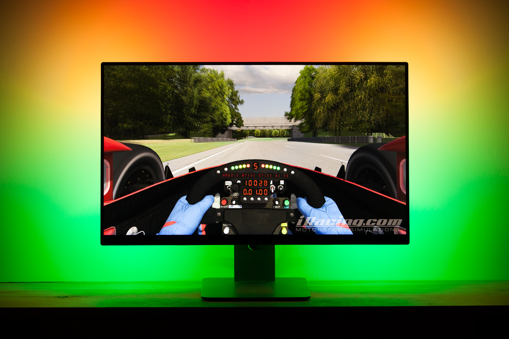
It feels great to finally get this cleaned up and put in place behind the monitor. Now the ambilight is completely hidden, and can be activated with few clicks on the PC.
I plan to make a Github repository for the PCB and case, just in-case anyone wants to create their own version of this project.
Next up: Part 6 – Adalight with FastLED